在现实中还原康威生命游戏:硬件极客打造实体触觉沙盒
文章背景与核心概要
康威生命游戏(Conway's Game of Life)是一个经典的零玩家游戏,仅凭简单的生死规则就能演化出极其复杂的行为。为了将这种数字世界的奇妙动态带入现实,一位硬件爱好者打造了一个包含 \(17\times17\) 矩阵的实体触觉版生命游戏装置。该项目巧妙地将交互艺术、PCB 电路设计和嵌入式固件工程结合在一起。
在硬件选型上,作者选用了成本高昂的 NKK 发光机械开关阵列,搭配 Microchip AVR128DA64 微控制器。通过多路复用(Multiplexing)技术、精心设计的 MOSFET 驱动电路以及高效的固件状态隔离策略,该设备在保证足够亮度的同时,实现了高可靠性的实时交互与仿真速度调节。最终,辅以精美的手工木制外壳,这个项目成为了一个集趣味性与技术性于一体的硬件杰作。
康威生命游戏简介
如果你还不太了解,康威生命游戏是在一个由方格构成的二维网格上进行的,每个方格代表一个细胞,状态分为存活(1)或死亡(0)。在每一轮迭代中,所有周围存活邻居少于两个的活细胞都会因为“饥饿”而死亡,而周围有四个或更多活细胞的则会死于“人口过剩”。最后,任何恰好有三个存活邻居的死细胞都会复活——这可以说是最高级的数字造物术了。
If you’re unfamiliar, Conway’s Game of Life takes place on a two-dimensional grid of square cells, where each cell is either alive (1) or dead (0). In each iteration, all live cells with fewer than two neighbors die of “starvation,” while those with four or more die of “overpopulation.” Finally, any dead cell that has exactly three living neighbors comes alive—digital necromancy at its finest.
这个“游戏”在传统意义上其实算不上游戏;你只需画出一个初始图案,然后静观其变。简单的规则催生出复杂的行为,这自然让许多极客为之着迷。虽然我对游戏本身算不上狂热,但我对交互艺术情有独钟,于是我决定打造一个实体版本。
The “game” isn’t really a game in the traditional sense; you simply draw an initial pattern and watch what happens. Simple rules lead to complex behaviors, which naturally fascinates many nerds. While not a massive fan of the game itself, I am a sucker for interactive art, so I decided to build a physical version.
硬件与预算
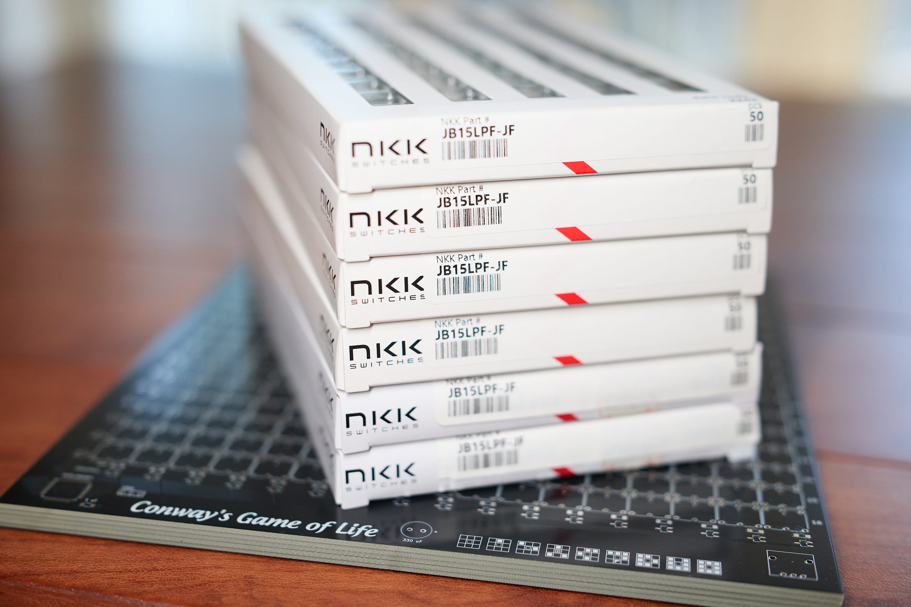
为了将这个想法付诸实践,我开始进行严格的预算规划:我先计算出项目合理的花费金额,然后将其乘以 10。这让我能够放手去采购 \(17\times17\) 矩阵的 NKK JB15LPF-JF 开关。以下是(字面意义上的)烧钱特写:
To bring the idea to life, I started with rigorous budgeting: I figured out what would be a reasonable amount to spend on the project and then multiplied that by 10. This allowed me to aim for a \(17\times17\) matrix of NKK JB15LPF-JF switches. Here’s the (literal) money shot:
PCB 设计与电路架构
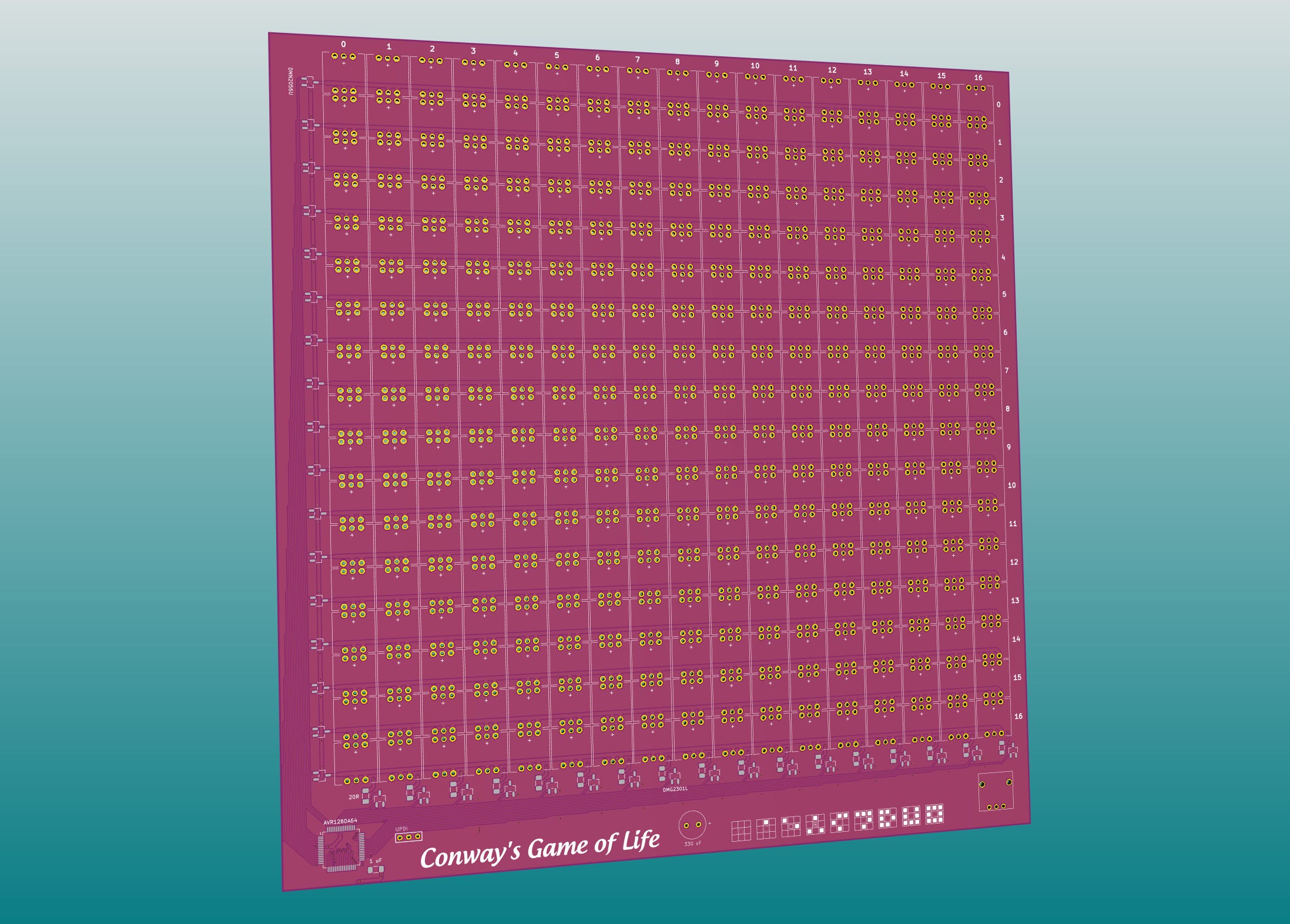
在等待开关到货的间隙,我完成了 PCB 的设计。这些开关占据了板子绝大部分的空间,不过在左下角刚好留出了足够的空间来容纳 Microchip 的 AVR128DA64 微控制器:
While waiting for the switches to arrive, I designed the PCB. The switches take up the vast majority of the board space, but there is just enough room for Microchip’s AVR128DA64 microcontroller tucked away in the bottom-left corner:
多路复用与电源管理
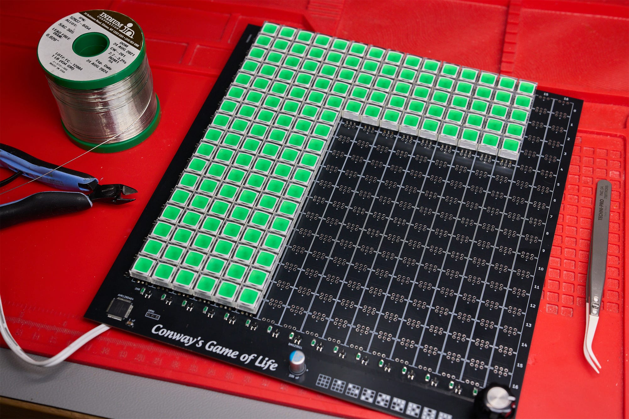
显示屏的控制方案非常直观。集成在开关中的 LED 呈 \(x\text{-}y\) 网格状排列: 1. 前 17 个 MCU GPIO 引脚将单个处于活动状态的 LED 行连接到地。 2. 随后的 17 个引脚向列提供正电压。
The control scheme for the display is straightforward. The switch-integrated LEDs are laid out in an \(x\text{-}y\) grid: 1. The first 17 MCU GPIO lines connect a single active LED row to ground. 2. The next 17 lines supply positive voltages to the columns.
由于采用了这种多路复用技术,每一行的占空比为 \(1/17\)(大约 \(6\%\))。为了保持足够的亮度,我通过向 LED 施加更高的电流来进行补偿。只要开关频率足够高以防止热结损坏,且平均电流保持在规范范围内,这样做就是安全的。
Because of this multiplexing, the duty cycle of each row is \(1/17\)th (roughly \(6\%\)). To maintain adequate brightness, I compensated by driving higher currents through the LEDs. This is safe as long as the switching frequency remains high enough to prevent thermal junction damage and the average current stays within specification.
电流由与列线串联的 \(20\,\Omega\) 电阻进行限制,从 \(5\text{ V}\) 电源轨向每个 LED 提供约 \(150\text{ mA}\) 的电流。如果整行都被点亮,总电流消耗将达到 \(2.5\text{ A}\),不过在正常情况下,大部分游戏区域都是黑暗的。
Current is limited by \(20\,\Omega\) resistors in series with the column lines, supplying about \(150\text{ mA}\) to each LED from a \(5\text{ V}\) rail. If an entire row is illuminated, total current consumption reaches \(2.5\text{ A}\), though under normal conditions most of the playfield remains dark.
由于每个二极管 \(150\text{ mA}\) 的电流超出了 MCU 引脚的安全承受范围,我引入了小型 N 沟道 MOSFET(DMN2056U)用于行切换,并使用互补的 P 沟道晶体管(DMG2301L)用于列线。
Since \(150\text{ mA}\) per diode exceeds what the MCU pins can safely handle, I incorporated small N-channel MOSFETs (DMN2056U) for row switching and complementary P-channel transistors (DMG2301L) for the column lines.
输入处理与固件设计
为了检测用户输入,我复用了行选通线,将各个开关组拉低到地,并额外布设了 17 个 GPIO 引脚来检测对应行的开关是否闭合。MCU 内部的上拉电阻处理了必要的偏置。
To detect user input, I reused the row-select lines to pull individual banks of switches to ground, routing another 17 GPIO pins to sense whether the switches in that row are closed. Internal pull-up resistors on the MCU handle the necessary biasing.
用户界面与速度控制
- 速度: 通过一个 \(10\,\text{k}\Omega\) 的电位器配合安装在右下角的高级旋钮(威世 ACCKIS2012NLD6)进行控制,并连接到一个 ADC 引脚。模拟运行速度从 \(0\) 到大约 \(10\text{ Hz}\) 可调。
- 编辑: 按下开关即可切换其细胞状态。每次按键都会使仿真暂停两秒钟,这样你就可以绘制多像素形状,而不用跟速度旋钮较劲。
User Interface and Speed Control
- Speed: Controlled via a \(10\,\text{k}\Omega\) potentiometer paired with a fancy knob (Vishay ACCKIS2012NLD6) mounted in the bottom-right corner and connected to an ADC pin. The simulation runs from \(0\) up to roughly \(10\text{ Hz}\).
- Editing: Pressing a switch toggles its cell state. Each keypress pauses the simulation for two seconds so you can draw multi-pixel shapes without fighting the speed knob.
固件可靠性
为了防止在屏幕刷新期间发生崩溃(这可能会维持 \(100\text{ mA}\) 的持续电流并烧毁二极管),显示逻辑与游戏逻辑完全解耦。状态评估发生在所有 LED 熄灭的短暂“黑暗”窗口期间。此外,如果主事件循环挂起超过 \(15\) 毫秒,微控制器内部的看门狗定时器将强制执行重启。
Firmware Reliability
To prevent crashes during screen refreshes—which could sustain the \(150\text{ mA}\) current and burn out diodes—the display logic is completely decoupled from the game logic. State evaluation occurs during a brief "blackout" window when all LEDs are switched off. Additionally, the microcontroller's internal watchdog timer forces a reboot if the main event loop hangs for more than \(15\text{ milliseconds}\).
成品展示
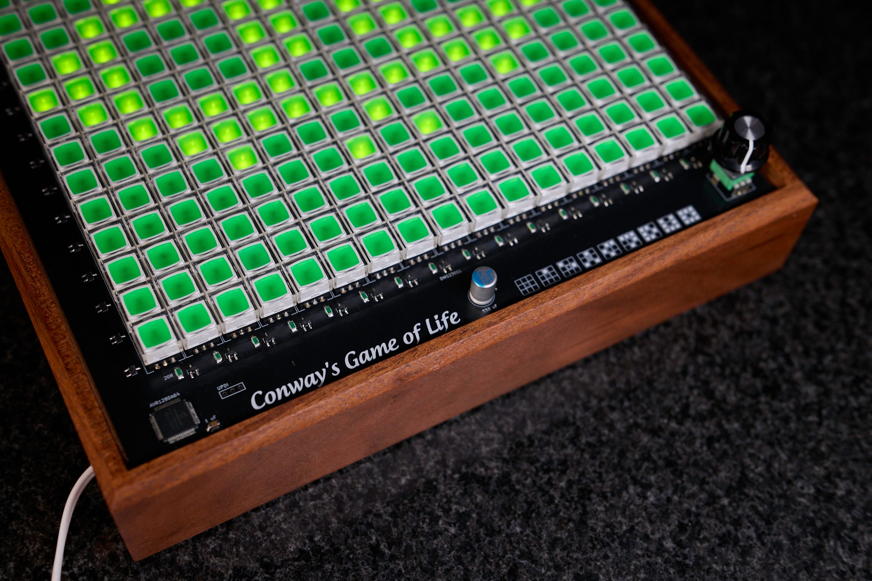
这是装入手工制作木质外壳中的成品设备的特写:
Here is a close-up of the completed device housed in a handcrafted wooden enclosure:
你还可以观看以下视频来欣赏设备的实际运行效果:
You can also watch the following video to see the device in action:
对于有兴趣自己动手的读者,源代码和 PCB 生产文件可以在这里找到。
For those interested in building their own, the source code and PCB production files can be found here.
还能以更低的成本制作吗?
这些发光开关每个售价约 3 美元,构成了大部分的成本。除非你在开关工厂有熟人(如果有的话,请介绍给我!),否则我想不出更便宜的方法。触控屏会更便宜,可以说功能也更完善,但它完全缺乏实体触控的满足感。
The illuminated switches cost around $3 a piece and make up the vast majority of the price tag. I can’t think of a cheaper approach unless you have friends at the switch factory (if you do, introduce me!). A touchscreen would be cheaper and arguably more functional, but it lacks all of the tactile satisfaction.
你可以选择更简单的开关和独立的 LED,然后通过 3D 打印或树脂浇筑定制键帽。然而,你在元器件上省下的钱,在设备、材料和时间上会加倍花出去。
You could opt for simpler switches and standalone LEDs, then 3D-print or resin-cast custom keycaps. However, whatever you save in components, you will spend thrice over in equipment, materials, and time.
反过来说,如果你想花更多的钱,做一个采用定制翻转点阵显示屏(Flip-dot display)的纯机电版本会是一个绝佳的项目——前提是你有很多钱,而且完全闲得发慌。
On the flip side, if you want to spend more, a fully electromechanical version using a custom flip-dot display would be a fantastic project if you have too much money and absolutely nothing else to do with your time.
📖 如果你喜欢这篇文章,你一定会喜欢 电路的秘密生活(The Secret Life of Circuits)。这是一本图文并茂、通俗易懂的电子学入门书——从导电物理学到嵌入式系统编程。它包含 290 多个彩色图表、420 多页原创内容,且完全没有 AI 参与。
📖 If you liked the article, you’ll enjoy The Secret Life of Circuits. It’s a richly illustrated, lucid introduction to electronics—from the physics of conduction to embedded system programming. It features 290+ color diagrams, 420+ pages of original content, and zero AI.
你可能也会喜欢:
You might also enjoy:
我撰写了大量关于极客文化、电子电路设计、算法等主题的深度原创文章。如果你喜欢这些内容,请订阅我。
I write well-researched, original articles about geek culture, electronic circuit design, algorithms, and more. If you like the content, please subscribe.